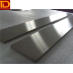
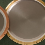
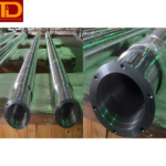
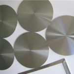
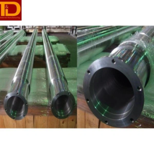
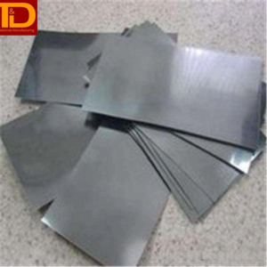
Tantalum Targets & Machined Parts
Sputtering targets made from high-purity steel gray tantalum metal boast exceptional qualities. Tantalum, a glossy bluish-gray transition metal, demonstrates remarkable corrosion resistance. Belonging to the refractory metal group, tantalum is frequently employed as a minor component in various alloys. Renowned for its dark hue, density, ductility, hardness, ease of manufacturing, and impressive thermal and electrical conductivity, tantalum is particularly acclaimed for its resistance to acid corrosion. Notably, at temperatures below 150°C, tantalum exhibits near-total immunity to regular aqua regia.
The production of Tantalum Sputtering Target involves electron beam (EB) melting. This type of sputtering target finds common applications in various industries, including magnetic recording media, printer components, flat panel displays, optics, industrial glass, and thin film resistors. In the semiconductor sector, high-purity Tantalum Sputtering Target is a preferred choice. Its inherent strength, coupled with a low thermal expansion coefficient, makes it ideal as a diffusion barrier. This is especially crucial in preventing unwanted interactions between copper and silicon, given tantalum’s unique ability to adhere to both materials.
T&D specializes in manufacturing Tantalum sputtering targets, offering a range of shapes and purities tailored for applications in the semiconductor and microelectronics industry. Our Tantalum sputtering targets stand out due to our unique forming processes, resulting in higher density, reduced average particle size, and elevated purity levels. This translates to expedited processes with increased sputtering speed, allowing for the production of exceptionally uniform Tantalum layers.
Our adaptable production process allows for an adjustable microstructure to achieve your specific desired outcomes. When the grains of the sputtering target are consistently aligned, users can experience steady erosion rates and uniform layers.
Chemical purity plays a pivotal role in a metal sputtering target. Higher purity levels result in films with superior electrical conductivity and minimized particle formation during the PVD process.
Analytical Methods:
- Metallic elements were analyzed by GDMS and ICP-OES.
- Gas elements were analyzed by LECO.

Preparation process of tantalum sputtering target
Preparation – Sintering – Vacuum Electron Beam Melting – Plastic Deformation – Annealing – Metallographic Inspection – Machining – Dimensional Inspection – Cleaning-Final Inspection – Packaging
Tantalum sputtering target manufacturing process
The manufacturing process primarily involves the initial sintering of high-purity tantalum powder to create a block. Subsequently, a high-vacuum electron beam melting furnace is utilized to produce a high-purity tantalum ingot. The tantalum ingot undergoes iterative plastic deformation and annealing to achieve a consistent crystal grain and a specific internal texture, resulting in a tantalum target blank. This target blank is welded to a back plate and further processed through machining to yield the final product. In this manufacturing approach, the high-purity tantalum powder undergoes sintering to form a block, followed by smelting into an ingot using a high-vacuum electron beam. The ingot then undergoes repeated plastic deformation and annealing processes, ultimately yielding a sputtering target suitable for semiconductor production.
Other alloy forms of tantalum sputtering target
Tantalum tungsten, tantalum niobium, tantalum aluminum, tantalum silicon, tantalum hafnium alloy sputtering target, etc.

